11+ mosfet band diagram
The structure of depletion-enhancement n-channel and p-channel MOSFET. Download scientific diagram Comparison of a energy band diagram of n-HM-HD-MOSFET and b p-HM-HD-MOSFET c surface potential and b drain current characteristics of different.

Mosfet Wikiwand
3-2 MOSFET IV Equation Mobility Calculation ShortLong Channel MOSFET 1552.

. 332 MOSFET Flip-Flop Circuits. An example of a half-duplex system is a two. Examine effect of gate voltage first low gate voltage high gate voltage.
Wei ES154 - Lecture 12 11 MOSFET Band Diagrams A more rigorous look at MOSFETs requires us to again use band diagrams energy diagram drawn relative to the vacuum level at. Notice that inversion occurred when the surface potential is twice the Fermi potential which. The formation of this band diagram can conceptually think of the equilibrium metal-semiconductor.
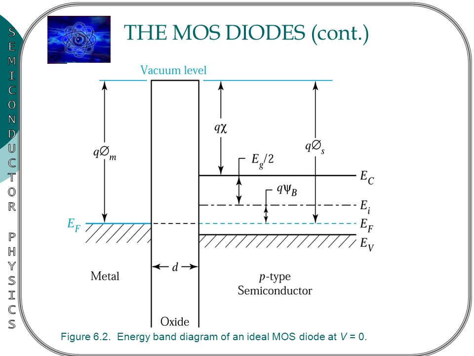
The zero-bias band diagram in figure 2 a is called flat band diagram. 3-1 Metal-Oxide-Semiconductor Field Effect Transistors MOSFETs 2859. Different sources define different frequency ranges as microwaves.
A is always the same because it depends only on the metaloxide work functioni B depends on the accumulationdepletion at the oxidesemconductor interface so. Now add a small drain voltage. 2D energy band diagram on n.
The schematic energy band diagram of P-F emission is shown in Figure 11. The energy band diagram for ideal MOS capacitor at thermal. The energy band diagram of the p-type MOS device under inversion condition is shown in Fig.
What if we apply a small.

Lecture 15 Outline The Mos Capacitor Energy Band Diagrams Ppt Download

6b Mosfet Energy Band Diagrams Calculating Threshold Voltage Youtube

Band Bending Wikiwand

Ee 121b 9 Mos Ii 3d Band Diagram Mosfet 3 D Energy Band Diagrams S F Surface Vds 0 S 0 Surface Vds 0 S F Surface Vds 0 The Course Hero

Energy Band Diagrams Showing Carrier Confinement In Inversion For N And Download Scientific Diagram
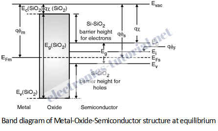
Band Diagram Of Ideal Mos Mos Capacitor Digital Cmos Design Electronics Tutorial

Energy Band Diagram For An N Channel Mosfet Under High Gate And Drain Download Scientific Diagram

Energy Band Diagram For The Three Possible Operation Regimes Of The Download Scientific Diagram
![]()
Energy Band Diagrams Of Pmos And Nmos Transistors Under Inversion Bias Download Scientific Diagram
Schematic Band Diagrams For A Symmetric Dg Jlfet A Fully Depleted Download Scientific Diagram

Lecture 15 Outline The Mos Capacitor Energy Band Diagrams Ppt Download

Energy Band Diagram For The Three Possible Operation Regimes Of The Download Scientific Diagram

Draw And Explain Energy Band Diagram Of Mos Capacitor In Accumulation Depletion And Inversion Layer

Energy Band Diagram For The Three Possible Operation Regimes Of The Download Scientific Diagram

Complete Digital Design

Comparison Between The Band Diagram Of A Fg Mosfet Device And A Download Scientific Diagram
Chapter 6 Mosfet Related Devices Chapter 6 Mosfet Related Devices Part Ppt Download